
In a groundbreaking development, researchers at Imec have discovered an innovative method to grow lasers directly on silicon. This advancement fundamentally addresses the longstanding challenges of integrating viable light sources with silicon photonics, which has limitations when it comes to generating light efficiently. The lasers developed utilize gallium arsenide, a material that does not naturally bond with silicon, thereby overcoming one of the major hurdles in the field of photonic chip manufacturing.
Table of Contents
- Challenges in Silicon Photonics
- Imec’s Breakthrough
- Technical Details of Laser Development
- Future Implications
Challenges in Silicon Photonics
Silicon photonics leverages light for data transmission, substantially improving data communication efficiency compared to traditional electrical methods. However, since silicon lacks the ability to effectively generate light on its own, it mandates the incorporation of lasers as a primary light source. Several complications arise from this necessity:
- Material Compatibility: The most effective laser materials, notably gallium arsenide (GaAs), do not bond easily with silicon.
- Cost Issues: Current approaches often involve complex bonding techniques, leading to high production costs and significant waste of raw materials.
- Performance Limitations: Existing methods can result in performance degradation due to defects arising during the integration of these distinct materials.
Imec’s Breakthrough
The research team at Imec, located in Belgium, has made a significant stride by devising a technique to grow lasers directly on silicon substrates. This revolutionary process is expected to lower costs while enhancing the scalability of photonic devices, potentially triggering advancements in fields such as artificial intelligence and telecommunications.
In a paper published in Nature, the researchers outline their novel approach, which employs nano-ridge engineering. This technique confines defects within the silicon structure, preventing them from adversely impacting the overall performance of the laser.
Technical Details of Laser Development
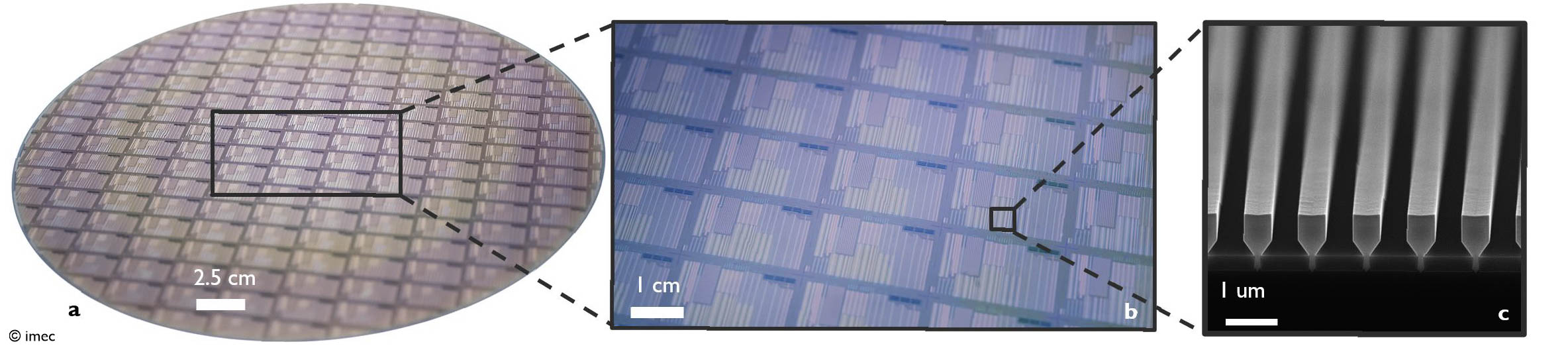
The methodology involves a meticulous process where a silicon wafer is first coated with a layer of silicon dioxide. Following this, arrowhead-shaped trenches are etched into the silicon surface, resembling a field prepared for planting. Subsequently, gallium arsenide is deposited into these trenches, ensuring that it only contacts the silicon at the bottom. This design effectively buries any potential defects, safeguarding the integrity of the laser material above.
The newly developed lasers leverage indium gallium arsenide (InGaAs) as the optical gain region. They are incorporated within a p-i-n diode structure and can operate at room temperature, achieving continuous-wave electrical injection with remarkably low threshold currents of just 5 mA and output powers reaching up to 1.75 mW.
Bernardette Kunert, scientific director at Imec, noted, “Over the past years, Imec has pioneered nano-ridge engineering, a technique that builds on selective-area growth (SAG) and aspect-ratio trapping (ART) to create low-defectivity III-V nano-ridges outside the trenches.” This innovation allows for the first full wafer-scale fabrication of electrically pumped GaAs-based lasers using standard 300 mm silicon wafers within a CMOS pilot manufacturing line.
Future Implications
The lasers developed by Imec emit light at a wavelength of 1,020 nanometers, which is shorter than wavelengths typically employed in telecommunications. Researchers are currently focusing on extending this wavelength while simultaneously refining the design to mitigate defects that may occur near electrical contacts. Should these efforts prove successful, the implications could be profound:
- Cost-Effective Solutions: This process holds the potential to significantly drive down costs associated with laser integration in silicon photonics.
- Enhanced Performance: By reducing defect densities, the optical performance of these lasers could vastly improve, facilitating more efficient data transmission.
- Scalability: The ability to fabricate lasers directly on silicon wafers opens avenues for high-volume production of advanced optical devices.
The research conducted at Imec represents a pivotal moment in the quest to enhance photonic integration, paving the way for the next generation of high-performance optical devices. As the boundaries of technology continue to expand, the implications of this work extend into critical applications across various sectors, including machine learning, AI, and telecommunications.
(Image credit: Imec)
Leave a comment